Image Analysis for the Microelectronics Industry
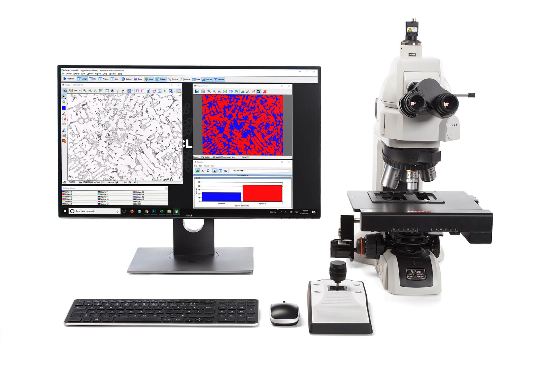
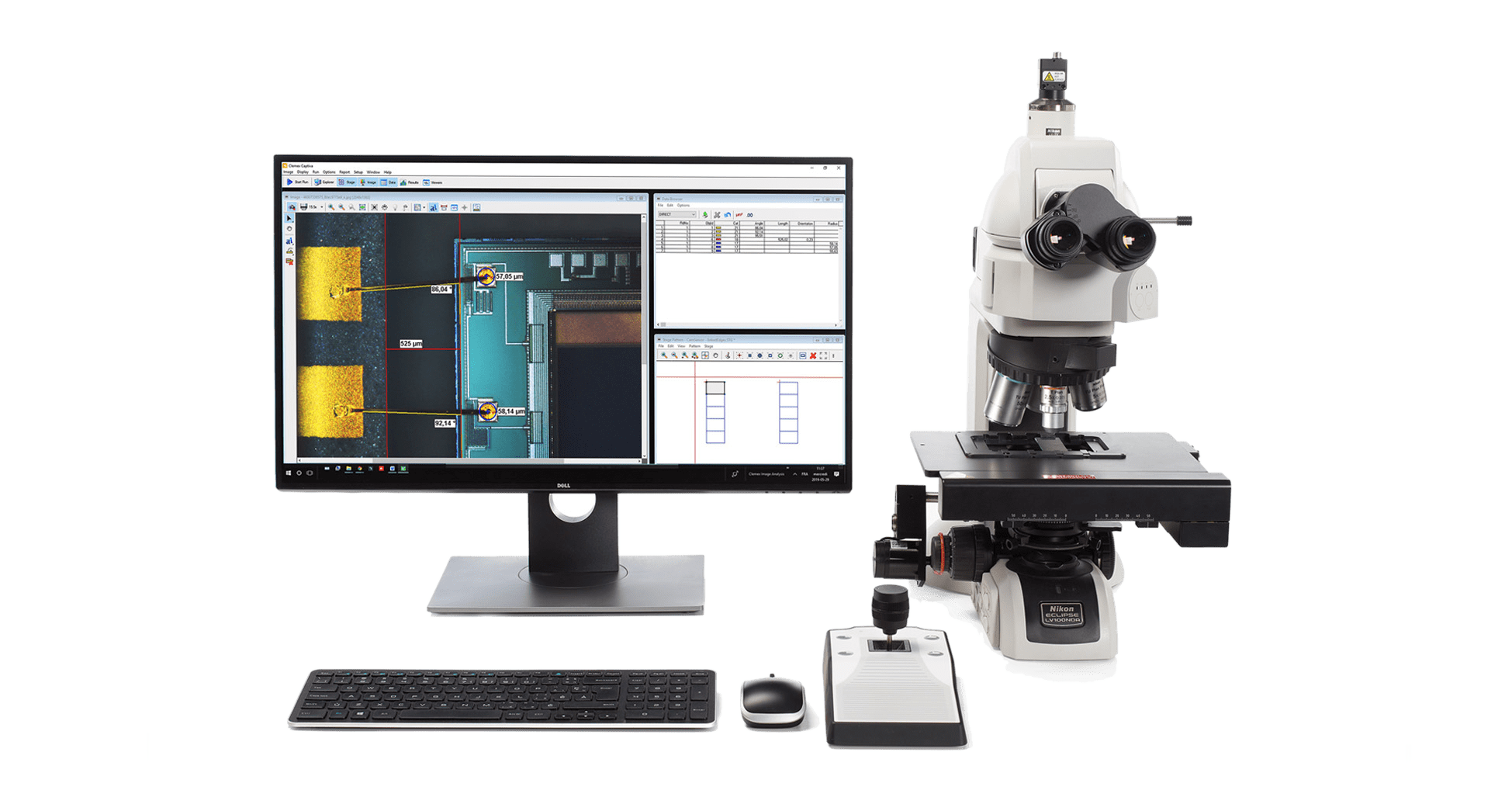
With our cutting-edge technology and expertise, we can solve the industry’s most challenging problems such as defect detection in semiconductor wafer inspection. We can inspect many types of surfaces and validate their integrity using the power of image analysis vision technologies and auto-stage controls.


APPLICATIONS
Our image analysis software is exceptionally flexible, allowing for any number of distinct routines to be run on the same system. These routines come packaged as a library of existing applications or can be developed by our applications specialists. Especially for the academic sector a wide variety of potable applications can be measured:
Various image analyses:
- Defect detection on wafers: etch pit count, area, worst field
- Detect vertically aligned plating lines and perform width measurements on chips
- Concentricity of foam insulator covering electric wire
SOLUTIONS